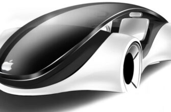
- Your iPhone Will Never Come With These 2 Things Ever Again
- No Charger in the Box? Everything You Need to Know About Charging the iPhone 12 and 13
- What Comes With the iPhone 12 and iPhone 13?
- How Do I Charge the iPhone 12 and iPhone 13?
- What Is MagSafe?
- What’s the Fastest Way to Charge the iPhone 13?
- Ken Shirriff’s blog
- Apple iPhone charger teardown: quality in a tiny expensive package
- How it works
- The circuit in detail
- The primary
- The secondary
- Isolation
- Schematic
- These circuits are very small
- Transformer teardown
- Apple’s huge profit margins
- Apple’s 2008 charger safety recall
- What makes Apple’s iPhone charger special
- Conclusions
- Notes and references
Your iPhone Will Never Come With These 2 Things Ever Again
Apple is addressing the waste problem, but it means you have to say goodbye to these freebies.
In the wake of Apple’s recent announcement about the new iPhone 12 and iPhone 12 Pro, you may have been so excited about your new phone that you didn’t hear that the company is making a big change that has some customers outraged. Sure, the new phones come with the largest display ever on an iPhone, a more durable front cover, and new technology that offers protection against everyday spills. Yes, there’s better photo quality, faster download and upload speed, higher quality video streaming, and a longer battery life. But there are two things your new iPhone won’t come with: a wall charger or headphones. Read on to find out why and what you need to know if you’re buying an iPhone soon. And for another major change from Apple, check out Apple Just Discontinued This Popular Phone.
Apple is framing this as part of the company’s drive towards sustainability. «Today, Apple is carbon neutral for global corporate operations and, by 2030, plans to have net zero climate impact across the entire business, which includes manufacturing supply chains and all product life cycles,» the company said in the announcement.
And that goal means removing unnecessary items from the phone packaging. Doing away with the power adaptor and earbuds means fewer carbon emissions, less mining of precious materials and a reduction in box size, which allows 70 percent more of them to be shipped on a pallet.
«Taken altogether, these changes will cut over 2 million metric tons of carbon emissions annually, equivalent to removing nearly 450,000 cars from the road per year,» Apple notes. And for another brand making a big change for the sake of the environment, find out What You’ll Never See in a Lego Box Set Again.
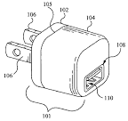
Nope. If you have one of those small square white chargers from Apple (called a brick) that has an ordinary USB plug on it (called a USB-A)—pictured here—you won’t be able to use that with the new cable Apple provides with the iPhone 12 models, CNBC notes. The new phones will ship with a USB-C to lightning cable, but previous phones used USB-A to lightning cables.
If you’ve gotten a newer iPad or Mac, they use similar USB-C to lightning cable plugs, so you may already have one at home.
You can always plug your new iPhone into your computer to charge. But if you don’t want to do that and don’t have a more recent charger from Apple, you’ll have to buy a new wall plug that’s compatible with the iPhone 12’s cable: Apple’s $20 20-watt iPhone plug. Other brands sell similar chargers for comparable prices or a little less.
Your other option is to buy Apple’s new MagSafe wireless charger, which uses «magnets [that] align themselves perfectly every time for faster wireless charging.» That will cost you $39.
The changes are going to apply retrospectively to other iPhones still on the market direct from Apple. iPhone XR, iPhone 11 and the 2020 iPhone SE will now ship with just the phone and the USB-C to lightning cable in the box.
If you’re interested in upgrading, both new iPhone 12 models are due for release Oct. 23 and can be pre-orderd from Apple now, with some network providers also offering pre-order and upgrade deals. And if you’re looking to save a little money on your phone expenses, This Is the Best Way to Lower Your Cell Phone Bill, Experts Say.
Источник
No Charger in the Box? Everything You Need to Know About Charging the iPhone 12 and 13
The latest Apple iPhones don’t ship with a power adapter, but they do support Apple’s wireless MagSafe charging. Whether you use a cable or not, these are the fastest ways to charge the iPhone 12 and iPhone 13.

Starting with iPhone 12, Apple no longer includes power adapters in every box as it moves to reduce package waste (and make some cash on accessories). Its newest smartphones also include support for Apple’s magnetic MagSafe charging. Here’s what you need to know about charging your iPhone 12 and iPhone 13, and what you might need to purchase.
What Comes With the iPhone 12 and iPhone 13?
Every iPhone 12 and iPhone 13 comes with a USB-C-to-Lightning cable, and that’s pretty much it. So out of the box, those who don’t currently have any Apple power adapters will need a USB-C power adapter to charge the iPhone 12 and 13.
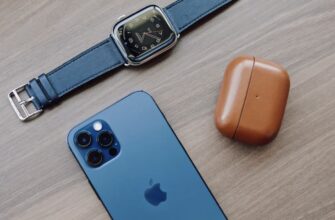
Plus, the newer iPhones ship without EarPods, so you’ll need to supply your own headphones to listen to music and podcasts. Apple sells its own AirPods wireless earbuds, but there are plenty of alternatives that won’t break the bank, not to mention our picks for best wireless headphones and those made with runners in mind.
As Apple explained during its iPhone 12 event last year, excluding the power adapter reduces the size of the box. This means 70% more devices can fit on a shipping pallet, which means more iPhone 12 devices can ship to users. Smaller boxes also allow Apple to reduce yearly carbon emissions by 2 million metric tons, it says.
How Do I Charge the iPhone 12 and iPhone 13?
Apple has not fully transitioned the iPhone to USB-C—which typically provides faster charging speeds—or removed ports altogether, so the iPhone 12 and iPhone 13 still include the typical Lightning charge port. This means you can use an existing Lightning cable and traditional USB-A power adapter to charge both phones. With the included USB-C-to-Lightning cable, though, you can also plug your iPhone into your Mac laptop.
Additionally, the iPhone 12 and iPhone 13 are compatible with current Qi wireless charging pads. However, Apple’s main focus for charging the iPhone 12 and 13 is its built-in, fast charging MagSafe magnetic power connector.
What Is MagSafe?
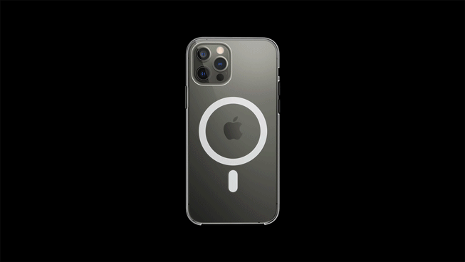
For years, Apple used the term MagSafe to describe its computers’ charging cable connectors. Their magnetized tips “snapped” into the magnetized MacBook charging ports—and snapped out if disturbed so as not to bring a Mac laptop crashing to the floor, for example. They disappeared a few years ago as Apple transitioned the MacBook lineup to USB-C charging and data transfer, but returned this fall in the M1 Pro/M1 Max-based MacBooks as «MagSafe 3.»
Apple brings a similar technology to the iPhone 12 and iPhone 13 lineup in the form of a magnetized “hockey puck” disc that looks like a big Apple Watch charger and snaps to the rear of the phone. This MagSafe connector includes a USB-C cord that plugs into a power source and charges at 15W.
What’s the Fastest Way to Charge the iPhone 13?
Since iPhone 5, Apple has shipped its iPhones with a 5W USB power adapter in the box, with the exception of the iPhone 11 Pro and Pro Max, which ship with an 18W USB-C power adapter. (Apple’s iPads also ship with 10W or 12W USB or 18W or 20W USB-C power adapters, depending on the model.) So unless the iPhone 12 or iPhone 13 is your first Apple device, you probably have one of them lying around.
Источник
Ken Shirriff’s blog
Computer history, restoring vintage computers, IC reverse engineering, and whatever
Apple iPhone charger teardown: quality in a tiny expensive package
How it works
In more detail, the AC line power is first converted to high voltage DC[1] by a diode bridge. The DC is switched on and off by a transistor controlled by a power supply controller IC. The chopped DC is fed into a flyback[2] transformer which converts it into low voltage AC. Finally, this AC is converted into DC which is filtered to obtain smooth power free of interference, and this power is output through the USB jack. A feedback circuit measures the output voltage and sends a signal to the controller IC, which adjusts the switching frequency to obtain the desired voltage.
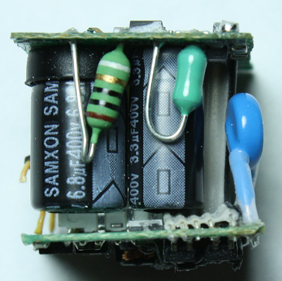
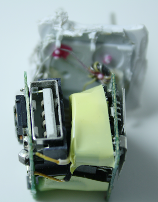
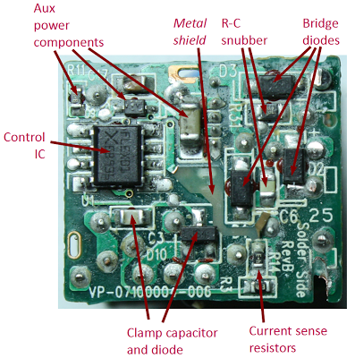
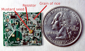
The side view above shows some of the larger components. The charger consists of two circuit boards, slightly under one inch square each.[3] The top board is the primary, which has the high voltage circuitry, and the bottom board, the secondary, has the low voltage output circuitry. The input AC first passes through a fusible resistor (striped), which will break the circuit if there is a catastrophic overload. The input AC is converted to high-voltage DC, which is smoothed by the two large electrolytic capacitors (black with white text and stripe) and the inductor (green).
Next, the high voltage DC is chopped at high frequency by a MOSFET switching transistor, which is the large three-pinned component in the upper left. (The second transistor clamps voltage spikes, as will be explained below.) The chopped DC goes to the flyback transformer (yellow, barely visible behind the transistors), which has low voltage output wires going to the secondary board below. (These wires were cut during disassembly.) The secondary board converts the low voltage from the transformer to DC, filters it, and then feeds it out through the USB connector (the silver rectangle in the lower left). The gray ribbon cable (just barely visible on the lower right under the capacitor) provides feedback from the secondary board to the controller IC to keep the voltage regulated.
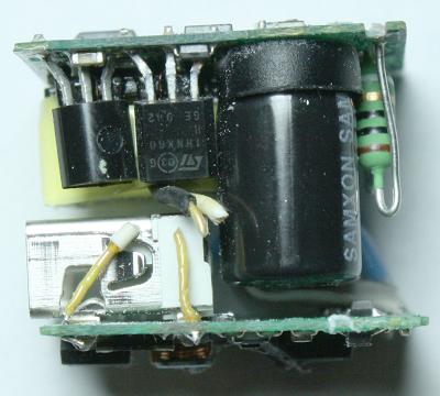
The picture above shows the flyback transformer (yellow) more clearly, above the USB jack. The large blue component is a special «Y» capacitor[4] to reduce interference. The controller IC is visible above the transformer on the top of the primary board.[5]
The circuit in detail
The primary
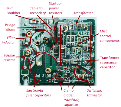
The primary circuit board is packed with surface mounted components on both sides. The inner side (diagram above) holds the large components while the outer side (diagram below) has the controller IC. (The large components were removed in the diagrams, and are indicated in italics.) Input power is connected to the corners of the board, goes through the 10Ω fusible resistor, and is rectified to DC by the four diodes. Two R-C snubber circuits absorb EMI interference created by the bridge.[6] The DC is filtered by the two large electrolytic capacitors and the inductor, producing 125-340V DC. Note the thickness of the circuit board traces connecting these capacitors and other high-current components compared to the thin control traces.
The power supply is controlled by an 8-pin STMicrosystems L6565 quasi-resonant SMPS controller chip.[7] The controller IC drives the MOSFET switching transistor which chops the high voltage DC and feeds it into the primary winding of the flyback transformer. The controller IC takes a variety of inputs (secondary voltage feedback, input DC voltage, transformer primary current, and transformer demagnetization sensing) and adjusts the switching frequency and timing to control the output voltage through complex internal circuitry. The current sense resistors let the IC know how much current is flowing through the primary, which controls when the transistor should be turned off.
The second switching transistor, along with some capacitors and diodes, is part of a resonant clamp circuit that absorbs voltage spikes on the transformer. This unusual and innovative circuit is patented by Flextronics.[8][9]
The controller IC needs DC power to run; this is provided by an auxiliary power circuit consisting of a separate auxiliary winding on the transformer, a diode, and filter capacitors. Since the controller IC needs to be powered up before the transformer can start generating power, you might wonder how this chicken-and-egg problem gets solved. The solution is the high-voltage DC is dropped to a low level through startup power resistors to provide the initial power to the IC until the transformer starts up. The auxiliary winding is also used by the IC to sense transformer demagnitization, which indicates when to turn on the switching transistor.[7]
The secondary
The USB output also has specific resistances connected to the data pins to indicate to the iPhone how much current the charger can supply, through a proprietary Apple protocol.[10] An iPhone displays the message «Charging is not supported with this accessory» if the charger has the wrong resistances here.
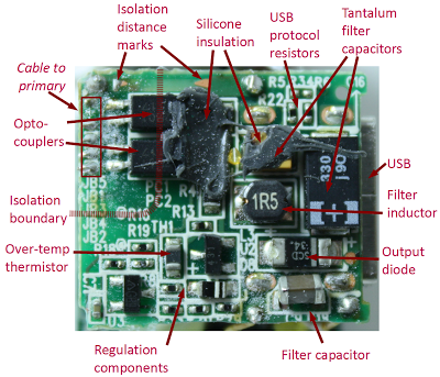
The secondary board contains a standard switching power supply feedback circuit that monitors the output voltage with a TL431 regulator and provides feedback to the controller IC through the optocoupler. A second feedback circuit shuts down the charger for protection if the charger overheats or the output voltage is too high.[11] A ribbon cable provides this feedback to the primary board.
Isolation
You might expect the primary board to have the dangerous voltages and the secondary board to have the safe voltages, but the secondary board consists of two areas: the hazardous area connected to the primary board, and the low-voltage area. The isolation boundary between these areas is about 6mm in the Apple charger and can be seen in the above diagram. This isolation boundary ensures that dangerous voltages cannot reach the output.
There are three types of components that cross the isolation boundary, and they must be specially designed for safety. The key component is the transformer, which provides a way for electrical power to reach the output without a direct electrical connection. Internally, the transformer is extensively insulated, as will be shown below. The second component type is the optocouplers, which send the feedback signal from the secondary to the primary. Internally, the optocoupler contains a LED and a photo-transistor, so the two sides are connected only by light, not by an electrical circuit. (Note the silicone insulation on the secondary side of the optocouplers to provide extra safety.) Finally, the Y capacitor is a special type of capacitor[4] that lets EMI (electromagnetic interference) escape between the high-voltage primary and the low-voltage secondary.
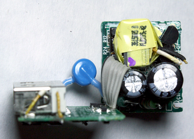
The above picture shows some of the isolation techniques. The secondary board (left) has the blue Y capacitor. Note the lack of components in the middle of the secondary board, forming an isolation boundary. The components on the right of the secondary board are connected to the primary board by the gray ribbon cable so they are at potentially high voltages. The other connection between the boards is the pair of wires from the flyback transformer (yellow) delivering the output power to the secondary board; these were cut to separate the boards.
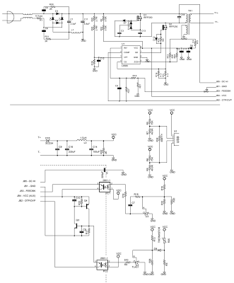
Schematic
These circuits are very small
Transformer teardown
The transformer measures roughly 1/2″ by 1/2″ by 1/3″. Inside, the transformer has three windings: a high voltage primary input winding, a low voltage auxiliary winding to provide power to the control circuits, and a high-current low voltage output winding. The output winding is connected to the black and white wires coming out of the transformer, while the other windings are connected to the pins attached to the bottom of the transformer.
The outside of the transformer has a couple layers of insulating tape. The second line appears to start with «FLEX», for Flextronics. Two grounded strands of wire are wrapped around the outside of the transformer to provide shielding.
![]()
After removing the shielding and the tape, the two halves of the ferrite core can be removed from the windings. Ferrite is a rather brittle ceramic material, so the core broke during removal. The core surrounds the windings and contains the magnetic fields. Each core piece is roughly 6mm x 11mm x 4mm; this style of core is known as EQ. The circular center section is very slightly shorter than the ends, creating a small air gap when the core pieces are put together. This 0.28mm air gap stores the magnetic energy for the flyback transformer.
![]()
Underneath the next two layers of tape is a 17-turn winding of thin varnished wire, which I think is another shield winding to return stray interference to ground.
![]()
Underneath the shield and another two layers of tape is the 6-turn secondary output winding that is connected to the black and white wires. Note that this winding is heavy-gauge wire, since it is feeding the 1A output. Also note that the winding is triple-insulated, which is a UL safety requirement to ensure that the high voltage primary remains isolated from the output. This is one place where cheap chargers cheat — they just use regular wire instead of triple-insulated, and also skimp on the tape. The result is there’s not much protecting you from high voltage if there’s an insulation flaw or power surge.
![]()
Under the next double layer of tape is the 11-turn heavy gauge primary power winding, that powers the controller IC. Since this winding is on the primary side, it doesn’t need to be triple insulated. It’s just insulated with a thin layer of varnish.
![]()
Under the final double layer of tape is the primary input winding, which is 4 layers of approximately 23 turns each. This winding receives the high voltage input. Since the current is very low, the wire can be very thin. Because the primary has about 15 times as many turns as the secondary winding, the secondary voltage will be 1/15 the primary voltage, but 15 times the current. Thus, the transformer converts the high voltage input to low voltage, high current output.
![]()
The final picture shows all the components of the transformer; left to right shows the layers from the outside tape to the innermost winding and bobbin.
![]()
Apple’s huge profit margins
Apple’s 2008 charger safety recall
In 2008, Apple recalled the iPhone chargers due to a defect that the AC prongs could fall off the charger and get stuck in an outlet.[15] The faulty chargers had the prongs attached with what was described as little more than glue and «wishful thinking».[15] Apple replaced the chargers with a redesigned model indicated by the green dot marking shown above (which counterfeit chargers inevitably imitate).
I decided to see what safety improvements Apple made in the replacement charger, and compare with other similar chargers. I tried pulling out the prongs of the Apple charger, a Samsung charger, and a counterfeit charger. The counterfeit prongs came out with a tug with pliers, as there’s basically nothing anchoring them but friction. The Samsung prongs took a lot of pulling and twisting with pliers, since they have little metal tabs holding them in place, but eventually they came out.
When I moved on to the Apple charger, the prongs didn’t budge, even with my hardest pulling with pliers, so I got out the Dremel and ground through the case to find out what was holding the prongs. They have large metal flanges embedded in the plastic of the case, so there’s no way a prong can come loose short of the destruction of the charger. The photo shows the Apple plug (note the thickness of plastic removed from the right half), the prong from the counterfeit charger held in only by friction, and the Samsung prong held in by small but sturdy metal tabs.
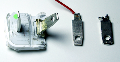
I’m impressed with the effort Apple put into making the charger more safe after the recall. They didn’t just improve the prongs slightly to make them more secure; clearly someone was told to do whatever it takes to make sure there’s absolutely no way the prongs could possibly come loose again under any circumstances.
What makes Apple’s iPhone charger special
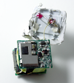
The input AC is filtered thorugh a tiny ferrite ring on the plastic case (see photo below). The diode bridge output is filtered by two large capacitors and an inductor. Two other R-C snubbers filter the diode bridge, which I’ve only seen elsewhere in audio power supplies to prevent 60Hz hum;[6] perhaps this enhances the iTunes listening experience. Other chargers I disassembled don’t use a ferrite ring and usually only a single filter capacitor. The primary circuit board has a grounded metal shield over the high-frequency components (see photo), which I haven’t seen elsewhere. The transformer includes a shield winding to absorb EMI. The output circuit uses three capacitors including two relatively expensive tantalum ones[14] and an inductor for filtering, when many supplies just use one capacitor. The Y capacitor is usually omitted from other designs. The resonant clamp circuit is highly innovative.[9]
Apple’s design provides extra safety in a few ways that were discussed earlier: the super-strong AC prongs, and the complex over-temperature / over-voltage shutdown circuit. Apple’s isolation distance between primary and secondary appears to go beyond the regulations.
Conclusions
If you’re interested in power supplies, please take a look at my other articles: tiny, cheap, dangerous: Inside a (fake) iPhone charger, where I disassemble a $2.79 iPhone charger and discover that it violates many safety rules; don’t buy one of these. Also take a look at Apple didn’t revolutionize power supplies; new transistors did which examines the history of switching power supplies. To see Apple’s adapter disassembled, check out videos created by scourtheearth and Ladyada. Finally, if you have an interesting charger lying around that you don’t want, send it to me and maybe I’ll write up a detailed teardown of it.
Also see comments on Hacker News.
Notes and references
[2] The Apple power supply uses a flyback design, where the transformer operates «backwards» from how you might expect. When a voltage pulse is sent into the transformer, the output diode blocks the output so there is no output — instead a magnetic field builds up. When the voltage input stops, the magnetic field collapses causing voltage output from the transformer. Flyback power supplies are very common for low-wattage power supplies.
[3] The primary board measures about 22.5mm by 20.0mm, while the secondary board is about 22.2mm by 20.2mm. [4] For more information on X and Y capacitors, see Kemet’s presentation and Designing low leakage current power supplies.
[5] For clarity, some insulation was removed before taking the pictures in this article. The Y capacitor was covered with black heat shrink tubing, there was tape around the side of the circuit, the fusible resistor was covered with black heat shrink tubing, and there was a black insulating cover over the USB connector.
[6] Snubber circuits can be used to reduce 60 Hz hum generated by the diode bridge in audio power supplies. A detailed reference on R-C snubbers for audio power supply diodes is Calculating Optimum Snubbers, and a sample design is An Audio Amplifier Power Supply Design.
[7] The power supply is controlled by the L6565 quasi-resonant SMPS (switched-mode power supply) controller chip (datasheet). (To be sure, the chip could be something else, but the circuit exactly matches the L6565 and no other chip I examined.)
To improve efficiency and reduce interference, the chip uses a technique known as quasi-resonance, which was first developed in the 1980s. The output circuit is designed so when the power is switched off, the transformer voltage will oscillate. When the voltage hits zero, the transistor switches back on. This is known as Zero Voltage Switching because the transistor is switched when there is essentially no voltage across it, minimizing wasted power and interference during switching. The circuit remains on for a variable time (depending on the power required), and then switches back off, repeating the process. (See Exploring quasi-resonant converters for power supplies for more information.)
One interesting consequence of quasi-resonance is the switching frequency varies depending on the load (with 70kHz as a typical value). Early power supplies such as the Apple II power supply used simple variable-frequency circuits to regulate the power. But in the 1980s, these circuits were replaced by controller ICs that switched at a fixed frequency, but varied the width of the pulses (known as PWM). Now, advanced controller ICs have gone back to variable frequency controls. But in addition, super-cheap knockoff power supplies use variable frequency circuits almost identical to the Apple II. So both high-end and low-end chargers are now back to variable frequency.
It took me a long time to realize that the «FLEX01» marking on the controller IC indicates Flextronics, and the X on the chip was from the Flextronics logo: . I assume the chip has these markings because it is being manufactured for Flextronics. The «EB936» marking on the chip could be Flextronics’ own part number, or a date code.
[8] I thought Flextronics was just an electronics assembler and I was surprised to learn that Flextronics does a lot of innovative development and has literally thousands of patents. I think Flextronics should get more credit for their designs. (Note that Flextronics is a different company than Foxconn, which manufactures iPads and iPhones and has the controversy over working conditions).
The picture above is from Flextronics Patent 7,978,489: Integrated Power Converters describes an adapter that looks just like the iPhone charger. The patent itself is a grab bag of 63 assorted claims (spring contacts, EMI shields, thermal potting material), most of which are not actually relevant to the iPhone charger.
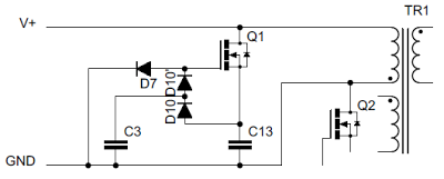
[9] Flextronics Patent 7,924,578: Two Terminals Quasi Resonant Tank Circuit describes the resonance circuit used in the iPhone charger, which is shown in the following diagram. Transistor Q2 drives the transformer. Transistor Q1 is the clamp transistor, which directs the voltage spike from the transformer into resonance capacitor C13. The innovative part of this circuit is that Q1 doesn’t need special drive circuitry like other active clamp circuits; it is self-powered via the capacitors and diodes. Most charger power supplies, by contrast, use a simple resistor-capacitor-diode clamp which dissipates the energy in the resistor.[18]
Later Flextronics patents extend the resonance circuit with even more diodes and capacitors: see patents 7,830,676, 7,760,519, and 8,000,112
[10] Apple indicates the charger type through a proprietary technique of resistances on the USB D+ and D- pins. For details on USB charging protocols, see my earlier references.
[11] One puzzling feature of the Apple charger is the second feedback circuit monitoring the temperature and output voltage. This circuit on the secondary board consists of a thermistor, a second 431 regulator, and a few other components to monitor the temperature and voltage. The output is connected through a second optocoupler to more circuitry on other side of the secondary board. Two transistors are wired in a SCR-like crowbar latch that will short out the auxiliary power and also shut down the controller IC. This circuit seems excessively complex for this task, especially since many controller ICs have this functionality built in. I could be misunderstanding this circuit, because it seems that Apple unnecessarily took up space and expensive components (maybe 25 cents worth) implementing this feature in such a complex way.
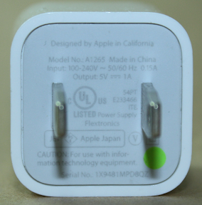
[12] Note the mysterious «For use with information technology equipment» on the outside of the charger. This indicates that the charger is covered by the safety standard UL 60950-1, which specifies the various isolation distances required. For a brief overview of isolation distances, see i-Spec Circuit Separation and some of my earlier references.
[13] Some notes on the components used: On the primary board, the JS4 package is two diodes in a single package. The input diodes labeled 1JLGE9 are 1J 600V 1A diodes. The switching transistors are 1HNK60 600V 1A N-channel MOSFETs. The values of many of the resistors and capacitors are indicated through standard SMD three-digit markings (two digits and then a power of ten, giving ohms or picofarads).
On the secondary board, the «330 j90» capacitor is a Sanyo POSCAP tantalum polymer 300mF 6.3V capacitor (j indicates 6.3V and 90 is a date code). 1R5 indicates a 1.5uH inductor. GB9 is a AS431I low cathode current adjustable precision shunt regulator, and 431 is a regular TL431 regulator. SCD34 is a 3A 40V schottky rectifier. YCW is an unidentified NPN transistor and GYW is an unidentified PNP transistor. The Y capacitor labeled «MC B221K X1 400V Y1 250V» is a 220pF Y capacitor. The «107A» capacitor is a 100 µF 10V tantalum capacitor (A indicates 10V). The optocouplers are PS2801-1. (All these component identifications should be considered tentative, along with the schematic.)
[14] In order to get a rough idea of how much the components in the charger cost, I looked up the prices of some components on octopart.com. These prices are the best prices I could find after a brief search, in quantities of 1000, attempting to match the parts accurately. I have to assume Apple’s prices are considerably better than these prices.
| Component | Price |
|---|---|
| 0402 SMD resistor | $0.002 |
| 0805 SMD capacitor | $0.007 |
| SMD transistor | $0.02 |
| fusible resistor | $0.03 |
| 1A 600V (1J) diode | $0.06 |
| thermistor | $0.07 |
| Y capacitor | $0.08 |
| 3.3uF 400V electrolytic capacitor | $0.10 |
| TL431 | $0.10 |
| 1.5uH inductor | $0.12 |
| SCD 34 diode | $0.13 |
| 2801 optocoupler | $0.16 |
| 1HNK60 transistor | $0.22 |
| USB jack | $0.33 |
| 100uF tantalum capacitor | $0.34 |
| L6565 IC | $0.55 |
| 330uF tantalum polymer capacitor (Sanyo POSCAP) | $0.98 |
| flyback transformer | $1.36 |
A few notes. Flyback transformers are generally custom and prices are all over the place, so I don’t have much confidence in that price. I think the POSCAP price is high because I was looking for the exact manufacturer, but tantalum capacitors are fairly expensive in general. It’s surprising how cheap SMD resistors and capacitors are: a fraction of a penny.
[15] Apple’s safety recall of chargers was announced in 2008. Blog reports showed that the prongs on the charger were attached only by 1/8″ of metal and some glue. Apple Recalls iPhone 3G Power Adapters in Wired provides more details.
[16] Low-quality chargers interfere with touchscreens, and this is described in detail in Noise Wars: Projected capacitance strikes back. (Customers also report touchscreen problems from cheap chargers on Amazon and other sites.)
[17] There are many industry designs for USB AC/DC converters in the 5W range. Sample designs are available from iWatt, Fairchild, STMicroelectronics, Texas Instruments, ON Semiconductor, and Maxim.
[18] When a diode or transistor switches, it creates a voltage spike, which can be controlled by a snubber or clamp circuit. For a lot of information on snubbers and clamps, see Passive Lossless Snubbers for High Frequency PWM Conversion and Switchmode Power Supply Reference Manual.
Источник